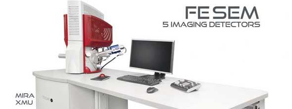
MIRA 3-XMU field emission scanning electron microscope
MIRA 3-XMU field emission scanning electron microscope is the newest and the most advanced FESEM in Iran and it provides users the advantages
of the latest technology. This microscope has the capability to provide topographical and elemental information at a magnification
of 1000000X by using four optical detectors (BSE-in beam, SE-in beam, SE, BSE). Another advantage of this device is related to LVSTD
detector which enables the possibility of shooting in very low voltages and hence the sample will be less damaged, it also makes it possible
to work on polymer materials, layers, and bio samples. It is also equipped with the second generation EDS microanalysis which is so small and
it allows to identify the smallest phases. Due to the possibility of adjusting the pressure inside the chamber and capability
of high-resolution, ability to work in all areas of science and industry, especially in the field of nano-technology is provided.